
As the demand for artificial intelligence (AI) and resource-intensive computing continues to surge, so too does the energy demand that accompanies these technological advancements. Researchers at the Massachusetts Institute of Technology (MIT) have risen to the challenge by developing an innovative technique for stacking transistors and memory directly on the back of computer chips. This groundbreaking approach holds the promise of significantly reducing energy costs associated with AI and high-performance computing.
Conventional chip designs have long hindered efficiency, primarily by separating logic and memory components. This traditional method forces data to shuttle back and forth between these distinct components, resulting in substantial inefficiencies and excessive energy consumption. MIT’s new technique not only addresses this inefficiency but also marks a significant leap towards more energy-efficient designs in future electronic devices.
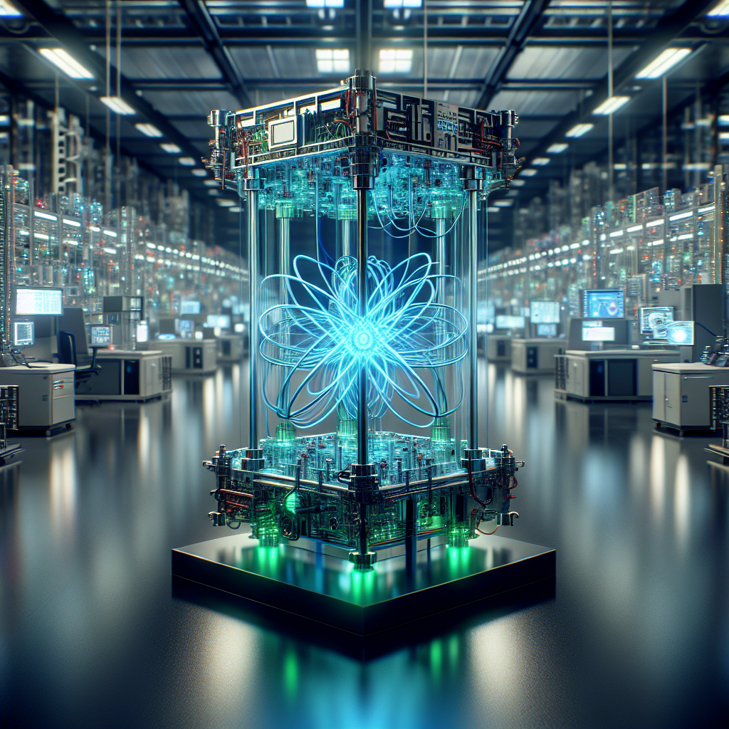
What sets this research apart is the new method’s ability to stack these vital components together on the backside of the chip, creating a more integrated and compact system. These developments contrast sharply with existing technologies such as Intel’s Lunar Lake and Apple’s M-series system-on-chips (SoCs), where sensitive transistors are built on one side of a silicon chip, leaving the opposite side reserved formally for wiring. As the complexity of adding more components grows, traditional fabrication approaches have struggled, primarily due to the prohibitive heat needed to fuse additional layers without damaging existing circuits.
MIT’s approach, spearheaded by researcher Yanjie Shao, overcomes these barriers through a novel low-temperature fabrication process. Utilizing a unique material known as amorphous indium oxide, the team successfully grew ultra-thin transistor layers at just 150 °C (302 °F). This temperature is sufficiently low to protect and preserve the integrity of the underlying circuits.
The breakthrough enables the stacking of active transistors directly onto the back end of the chip, merging both logic and memory functionalities into a single, compact vertical stack. This approach not only conserves space but enhances energy efficiency, paving the way for versatile electronics in ever-smaller devices. “Now, we can build a platform of versatile electronics on the back end of a chip that enables us to achieve high energy efficiency and many different functionalities in very small devices,” Yanjie Shao emphasized. However, he also noted the importance of continued innovation to fully uncover the ultimate performance limits of this promising technology.
Furthermore, the research team has improved upon existing transistor designs by incorporating a ferroelectric material known as hafnium-zirconium-oxide to formulate 20-nanometer transistors. Initial testing of these devices has shown remarkable results, with exceptionally swift switching speeds recorded at just 10 nanoseconds. Notably, this is the limit of the measurement equipment used by the team, indicating the impressive potential of their newfound designs.
The implications of this research extend beyond just technical specifications; the potential commercial upside is considerable. As industries increasingly rely on more powerful AI systems and data-driven technologies, lowering their energy consumption could translate into significant cost savings and improved sustainability practices. For business leaders, product developers, and investors, the advancement of MIT’s new transistor stacking technique represents a noteworthy step toward resolving the growing energy concerns surrounding AI applications.
In conclusion, the groundbreaking work being done at MIT not only showcases a novel fabrication technique that stacks transistors and memory but also reinforces the crucial relationship between energy efficiency and technological advancement. This innovation aligns with the general direction of the electronics industry, which seeks to develop more capable systems that are environmentally friendly and economically viable for future applications. As researchers continue to push the boundaries of performance and efficiency, the developments at MIT may very well shape the future landscape of AI and hybrid computing technologies.
Leave a Reply